- 您现在的位置:买卖IC网 > Sheet目录3841 > PIC16C63A-04I/SO (Microchip Technology)IC MCU OTP 4KX14 PWM 28SOIC
138
SAM7S Series [DATASHEET]
6175M–ATARM–26-Oct-12
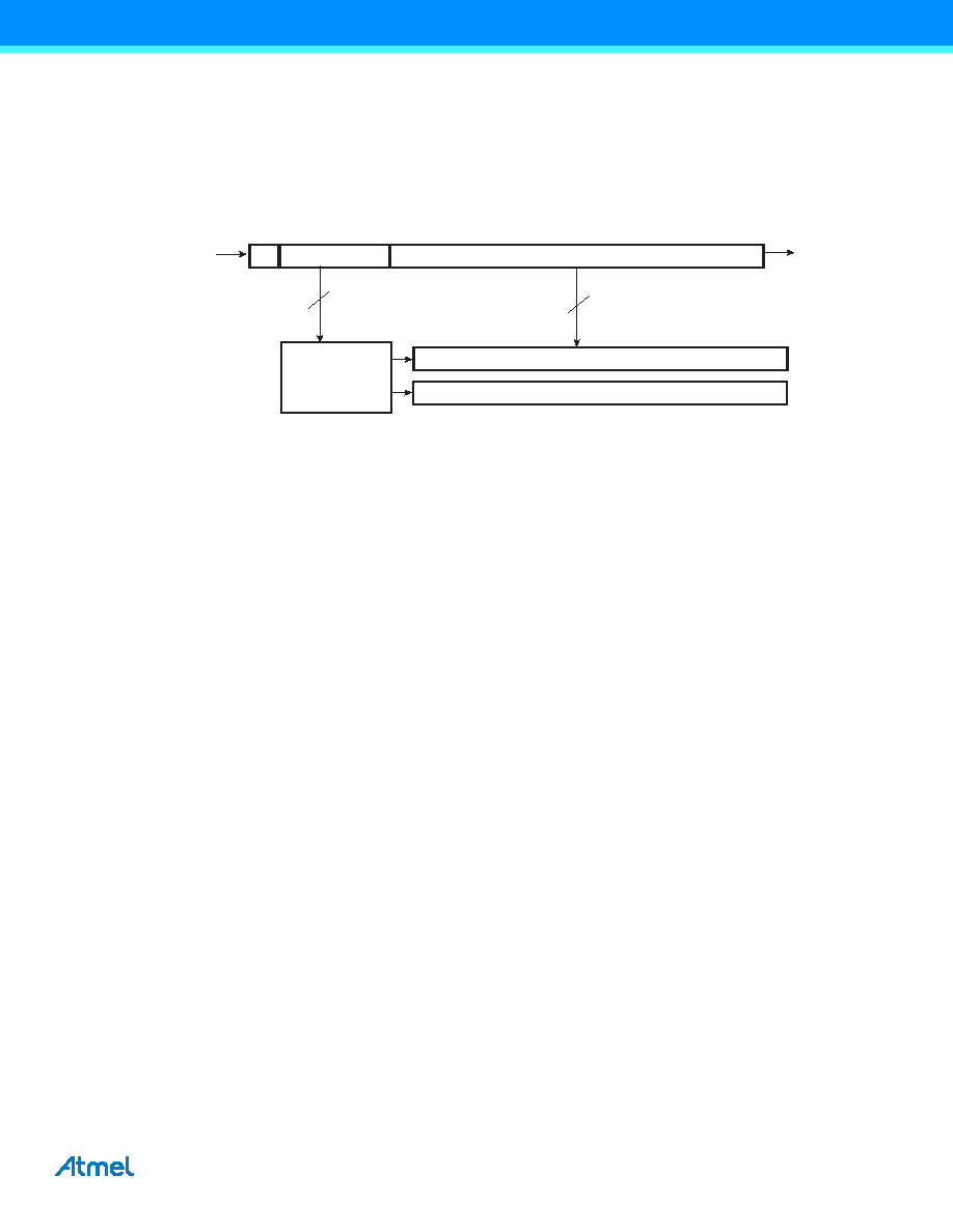
Access to these registers is done through the TAP 38-bit DR register comprising a 32-bit data field, a 5-bit address
field and a read/write bit. The data to be written is scanned into the 32-bit data field with the address of the register
to the 5-bit address field and 1 to the read/write bit. A register is read by scanning its address into the address field
and 0 into the read/write bit, going through the UPDATE-DR TAP state, then scanning out the data.
Refer to the ARM7TDMI reference manuel for more information on Comm channel operations.
Figure 20-8. TAP 8-bit DR Register
A read or write takes place when the TAP controller enters UPDATE-DR state. Refer to the IEEE 1149.1 for more
details on JTAG operations.
The address of the Debug Comms Control Register is 0x04.
The address of the Debug Comms Data Register is 0x05.
The Debug Comms Control Register is read-only and allows synchronized handshaking between the processor
and the debugger.
– Bit 1 (W): Denotes whether the programmer can read a data through the Debug Comms Data Register.
If the device is busy W = 0, then the programmer must poll until W = 1.
– Bit 0 (R): Denotes whether the programmer can send data from the Debug Comms Data Register. If R
= 1, data previously placed there through the scan chain has not been collected by the device and so
the programmer must wait.
The write handshake is done by polling the Debug Comms Control Register until the R bit is cleared. Once cleared,
data can be written to the Debug Comms Data Register.
The read handshake is done by polling the Debug Comms Control Register until the W bit is set. Once set, data
can be read in the Debug Comms Data Register.
20.3.4
Device Operations
Several commands on the Flash memory are available. These commands are summarized in Table 20-3 on page
126. Commands are run by the programmer through the serial interface that is reading and writing the Debug
Comms Registers.
TDI
TDO
4
0
r/w
Address
31
Data
0
Address
Decoder
Debug Comms Control Register
Debug Comms Data Register
32
5
发布紧急采购,3分钟左右您将得到回复。
相关PDF资料
52559-2270
CONN FFC 22POS .5MM VERT ZIF SMD
52559-1870
CONN FFC 18POS .5MM VERT ZIF SMD
DSPIC33EP64MC506-I/PT
IC DSC 16BIT 64KB FLASH 64TQFP
52745-1896
CONN FFC 18POS .5MM R/A ZIF SMD
PIC16LC622-04/P
IC MCU OTP 2KX14 COMP 18DIP
PIC16LF84A-04/P
IC MCU FLASH 1KX14 EE 18DIP
DSPIC30F1010-30I/MM
IC DSPIC MCU/DSP 6K 28QFN
52745-1696
CONN FFC 16POS .5MM R/A ZIF SMD
相关代理商/技术参数
PIC16C63A-04I/SP
功能描述:8位微控制器 -MCU 7KB 192 RAM 22 I/O RoHS:否 制造商:Silicon Labs 核心:8051 处理器系列:C8051F39x 数据总线宽度:8 bit 最大时钟频率:50 MHz 程序存储器大小:16 KB 数据 RAM 大小:1 KB 片上 ADC:Yes 工作电源电压:1.8 V to 3.6 V 工作温度范围:- 40 C to + 105 C 封装 / 箱体:QFN-20 安装风格:SMD/SMT
PIC16C63A-04I/SS
功能描述:8位微控制器 -MCU 7KB 192 RAM 22 I/O RoHS:否 制造商:Silicon Labs 核心:8051 处理器系列:C8051F39x 数据总线宽度:8 bit 最大时钟频率:50 MHz 程序存储器大小:16 KB 数据 RAM 大小:1 KB 片上 ADC:Yes 工作电源电压:1.8 V to 3.6 V 工作温度范围:- 40 C to + 105 C 封装 / 箱体:QFN-20 安装风格:SMD/SMT
PIC16C63A04SP
制造商:MICROCHIP 功能描述:NEW
PIC16C63A-20/SO
功能描述:8位微控制器 -MCU 7KB 192 RAM 22 I/O RoHS:否 制造商:Silicon Labs 核心:8051 处理器系列:C8051F39x 数据总线宽度:8 bit 最大时钟频率:50 MHz 程序存储器大小:16 KB 数据 RAM 大小:1 KB 片上 ADC:Yes 工作电源电压:1.8 V to 3.6 V 工作温度范围:- 40 C to + 105 C 封装 / 箱体:QFN-20 安装风格:SMD/SMT
PIC16C63A-20/SP
功能描述:8位微控制器 -MCU 7KB 192 RAM 22 I/O RoHS:否 制造商:Silicon Labs 核心:8051 处理器系列:C8051F39x 数据总线宽度:8 bit 最大时钟频率:50 MHz 程序存储器大小:16 KB 数据 RAM 大小:1 KB 片上 ADC:Yes 工作电源电压:1.8 V to 3.6 V 工作温度范围:- 40 C to + 105 C 封装 / 箱体:QFN-20 安装风格:SMD/SMT
PIC16C63A-20/SP
制造商:Microchip Technology Inc 功能描述:8 Bit Microcontroller Clock Speed:20MHz
PIC16C63A-20/SS
功能描述:8位微控制器 -MCU 7KB 192 RAM 22 I/O RoHS:否 制造商:Silicon Labs 核心:8051 处理器系列:C8051F39x 数据总线宽度:8 bit 最大时钟频率:50 MHz 程序存储器大小:16 KB 数据 RAM 大小:1 KB 片上 ADC:Yes 工作电源电压:1.8 V to 3.6 V 工作温度范围:- 40 C to + 105 C 封装 / 箱体:QFN-20 安装风格:SMD/SMT
PIC16C63A-20E/SO
功能描述:8位微控制器 -MCU 7KB 192 RAM 22 I/O RoHS:否 制造商:Silicon Labs 核心:8051 处理器系列:C8051F39x 数据总线宽度:8 bit 最大时钟频率:50 MHz 程序存储器大小:16 KB 数据 RAM 大小:1 KB 片上 ADC:Yes 工作电源电压:1.8 V to 3.6 V 工作温度范围:- 40 C to + 105 C 封装 / 箱体:QFN-20 安装风格:SMD/SMT